
In today’s data-driven enterprise landscape, organizations generate massive volumes of log data from applications, systems, and infrastructure components. Managing this information effectively requires robust logging pipeline solutions that can collect, process, store, and analyze log data efficiently. While cloud-based solutions have gained popularity, many enterprises continue to rely on on-premises logging pipeline solutions for various compelling reasons including data sovereignty, compliance requirements, and cost considerations.

AI-Driven E-Learning Personalization Tools: Revolutionizing Digital Education Through Intelligent Adaptation
The landscape of digital education has undergone a dramatic transformation in recent years, with artificial intelligence emerging as the driving force behind truly personalized learning experiences. As educational institutions and corporate training programs seek more effective ways to engage learners and improve outcomes, AI-driven e-learning personalization tools have become the cornerstone of modern educational technology.

Managed Web Application Firewalls: Complete Guide to Enhanced Cybersecurity Protection
In today’s digital landscape, where cyber threats evolve at an unprecedented pace, organizations face an increasingly complex challenge in protecting their web applications. Managed Web Application Firewalls (WAF) have emerged as a critical defense mechanism, offering businesses a sophisticated shield against malicious attacks while maintaining optimal performance and user experience.

Complete Guide to Virtual Machine Monitoring Tools: Essential Solutions for Modern IT Infrastructure
Virtual machine monitoring has become a critical component of modern IT infrastructure management. As organizations increasingly rely on virtualized environments to optimize resource utilization and reduce costs, the need for comprehensive monitoring solutions has never been more pressing. Understanding the landscape of virtual machine monitoring tools is essential for IT professionals seeking to maintain optimal performance, ensure security, and minimize downtime.

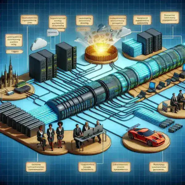
Distributed RAG Knowledge Systems: Revolutionizing Information Retrieval and AI-Powered Decision Making
In the rapidly evolving landscape of artificial intelligence and machine learning, Distributed RAG Knowledge Systems have emerged as a groundbreaking solution that’s reshaping how organizations handle vast amounts of information. These sophisticated architectures combine the power of Retrieval-Augmented Generation (RAG) with distributed computing principles, creating unprecedented opportunities for scalable, intelligent information processing.

The Ultimate Guide to TikTok Video Downloaders: Everything You Need to Know
In the rapidly evolving digital landscape, TikTok has emerged as one of the most influential social media platforms, captivating billions of users worldwide with its short-form video content. As users become increasingly engaged with the platform’s creative offerings, the demand for reliable methods to save and share favorite videos has grown exponentially. This comprehensive guide explores the world of TikTok video downloaders, providing insights into their functionality, legality, and practical applications.
YouTube TV’s Last-Minute Carriage Deals and the New Sports Streaming Bargaining Chips
YouTube TV has emerged as a significant player in the streaming industry, especially when it comes to live sports. In recent years, the platform has engaged in numerous last-minute carriage deals that highlight its aggressive approach to securing content. These deals are not just about acquiring channels; they also represent a shifting paradigm in how streaming services negotiate rights. Understanding these dynamics is crucial for both consumers and industry stakeholders.
Bagaimana Menghubungkan Tablet ke Komputer?
Menghubungkan tablet ke komputer mungkin tampak sebagai tugas yang sederhana, tetapi ada berbagai metode yang bisa digunakan, tergantung pada kebutuhan Anda. Baik Anda ingin mentransfer file, mensinkronisasi data, atau menggunakan tablet sebagai monitor tambahan, memilih metode yang tepat sangat penting. Artikel ini akan membahas beberapa cara efektif untuk menghubungkan tablet ke komputer dan manfaat dari setiap metode.
Dell Introduces Cloud-Native PCs Designed for AI-Heavy Workloads
As technology continues to evolve at a rapid pace, the need for powerful computing solutions has never been more critical. Dell has stepped into the spotlight with its latest innovation: cloud-native PCs designed specifically for AI-heavy workloads. These machines are set to redefine the way businesses and professionals approach artificial intelligence, machine learning, and data-intensive applications.

La Inteligencia Artificial en el Futuro del Trabajo: Transformación Digital y Nuevas Oportunidades Laborales
La inteligencia artificial está redefiniendo fundamentalmente la naturaleza del trabajo tal como la conocemos. Esta transformación tecnológica no es simplemente una tendencia pasajera, sino una revolución que está alterando profundamente las estructuras laborales, creando nuevas profesiones y modificando las competencias requeridas en prácticamente todos los sectores económicos.

IA para Automatizar Tareas Cotidianas: Revolucionando la Productividad Diaria
La inteligencia artificial (IA) ha dejado de ser un concepto futurista para convertirse en una realidad tangible que está transformando radicalmente la manera en que gestionamos nuestras actividades diarias. Desde despertar por la mañana hasta organizar nuestro tiempo libre, la IA para automatizar tareas cotidianas se ha posicionado como una herramienta indispensable para optimizar la productividad y simplificar nuestras vidas.
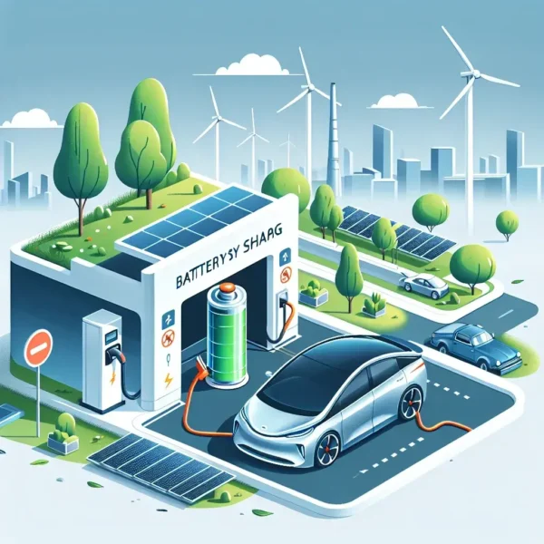
Honda Unveils EV Battery Swap Stations for U.S. Fleet Operators
In a significant move towards sustainable transportation, Honda has recently unveiled its plans to introduce EV battery swap stations tailored for U.S. fleet operators. As electric vehicles (EVs) gain traction in various sectors, the need for efficient battery management systems becomes increasingly crucial. This article delves into Honda’s initiative, exploring its potential impact on the future of fleet operations and the broader EV industry.

Paramount+ Introduces Ad-Supported Free Tier for Select U.S. Regions
In a significant move that is set to reshape the streaming landscape, Paramount+ has officially announced the launch of an ad-supported free tier in select regions across the United States. This game-changing initiative is designed to expand its viewer base by providing free access to its rich library of content, albeit with advertisements. As the streaming wars continue to heat up, this innovative approach places Paramount+ firmly in the spotlight, inviting both new and existing users to experience its offerings without the commitment of a subscription fee.

Public Schools Distribute Privacy Report Cards for EdTech Vendors Under New DOE Mandate
In an era where technology is deeply intertwined with education, the importance of student privacy cannot be overstated. Recent developments have led to public schools distributing privacy report cards for EdTech vendors under a new Department of Education (DOE) mandate. This initiative aims to enhance transparency and accountability in the use of educational technology, ensuring that student data is protected while fostering an environment conducive to learning.

AI Powered Cryo Robots Preserving Human Organs for Transplantation
In the ever-evolving landscape of medical technology, AI powered cryo robots are emerging as a groundbreaking solution for organ preservation, particularly for transplantation purposes. This innovative technology not only enhances the viability of human organs but also promises to alleviate the critical shortage of organs available for transplant. This article delves into the intricate workings of these advanced cryo robots, their significance, and the future they hold in the field of medicine.

Comcast Piloting AI Powered Smart Grid Connectivity in U.S. Homes
As technology continues to revolutionize the way we live, the integration of artificial intelligence (AI) into our daily operations is becoming increasingly prevalent. One of the most exciting developments in this realm is Comcast’s pilot program aimed at enhancing smart grid connectivity in U.S. homes. This initiative not only marks a significant step toward modernizing energy consumption but also showcases the potential for AI to play a pivotal role in our homes.

U.S. Navy Testing Robotic Submarines Guided by AI This September
As technology rapidly evolves, the military sector is not left behind in harnessing the capabilities of artificial intelligence (AI) and robotics. This September, the U.S. Navy is set to conduct significant tests of robotic submarines guided by AI. These advances promise to reshape the future of maritime defense and significantly enhance operational efficiency.

U.S. Court Ruling on Biometric Privacy Lawsuit Against Major Tech Firm This Month
This month, a pivotal ruling from a U.S. court has set the stage for an ongoing debate about biometric privacy in the tech industry. The lawsuit, which targets a major tech firm, has ignited conversations surrounding the ethical use of biometric data and the protection of individual privacy rights.

Zeemo YouTube Video Downloader: Complete Guide to Video Downloading and Subtitle Management
The digital landscape has transformed how we consume and share video content. With billions of hours of video uploaded to platforms daily, the need for reliable downloading solutions has become paramount. Content creators, educators, and casual users alike seek tools that can help them access videos offline while maintaining quality and adding valuable features like subtitle management.

Microsoft Teams Copilot Now Generates Meeting Action Items
In the fast-paced world of remote work and digital collaboration, teams are constantly seeking ways to enhance productivity. One of the most exciting developments in this area is the introduction of Microsoft’s AI-driven feature, Teams Copilot, which now generates meeting action items. This capability is set to transform the way teams operate, making meetings more efficient and outcomes more actionable.

MediaTek Dimensity 9400 to Debut in Q4 Flagship Phones
As the smartphone industry continues to evolve, chip manufacturers are racing to develop processors that can support the ever-increasing demand for performance, efficiency, and advanced features. Among them, MediaTek has made significant strides, with its latest offering, the Dimensity 9400, set to debut in flagship smartphones by the end of Q4 2023. This article delves into the anticipated features, expected devices, and the impact of this cutting-edge chip on the smartphone market.

Cybersecurity Insurance Premiums Rise 200% Following Major Corporate Breaches
In recent years, the landscape of cybersecurity has dramatically changed. With major corporate breaches making headlines globally, businesses are witnessing a seismic shift in their approach to cybersecurity insurance. Recent reports indicate that cybersecurity insurance premiums have surged by an astonishing 200% following a series of high-profile data breaches. This article delves into the factors driving this increase, its implications for businesses, and what the future may hold for cybersecurity insurance.

Edge Computing Infrastructure Reduces Latency for Mission-Critical Applications
In an era where speed and efficiency define success, edge computing is transforming the way organizations manage their data processing needs. By bringing computation closer to the data source, edge computing minimizes latency, which is crucial for mission-critical applications. This article delves into how edge computing infrastructure reduces latency, its implications for various industries, and its future prospects.

How Can I Clean Internal PC Fans to Prevent Overheating?
Overheating is one of the primary concerns for PC users, particularly gamers and professionals who rely heavily on their machines. A significant factor contributing to overheating is dust accumulation in internal components, especially the fans. Cleaning your internal PC fans is essential for maintaining airflow, optimizing performance, and prolonging the lifespan of your hardware. This article will guide you through the steps required to effectively clean your internal PC fans and prevent overheating.

The Complete Guide to Instagram Story Viewers: Understanding Privacy, Tools, and Digital Ethics
In today’s digital landscape, Instagram Stories have become a cornerstone of social media interaction, offering users a way to share ephemeral content that disappears after 24 hours. However, with this feature comes a natural curiosity about who’s viewing our content and, conversely, the desire to view others’ stories without leaving a digital footprint. This comprehensive exploration delves into the fascinating world of Instagram story viewing, examining the tools, ethics, and implications surrounding anonymous story consumption.

Revolutionizing Agriculture: Autonomous Agricultural Robots for Planting and Harvesting
The agricultural sector is undergoing a significant transformation, driven largely by advancements in technology. Among these innovations, autonomous agricultural robots are gaining prominence for their potential to enhance efficiency in planting and harvesting. This article delves into the mechanisms, advantages, challenges, and future outlook of these robotic systems.

How Solar Energy in Orbit Avoids Terrestrial Cooling Needs
Solar energy has long been recognized as a clean and renewable energy source, but its potential extends beyond terrestrial applications. With the advent of advanced space technologies, harnessing solar energy in orbit presents a groundbreaking opportunity to address several global challenges, including terrestrial cooling needs. This article delves into the mechanisms, advantages, and future possibilities of using solar energy from space, including its impact on climate control.

Community Notes: How Social Media’s Collaborative Fact-Checking Is Reshaping Information Verification
In today’s fast-paced digital landscape, information spreads at unprecedented speeds across social media platforms. As content proliferates, so does misinformation, creating an urgent need for effective fact-checking mechanisms. Traditionally, fact-checking was conducted by dedicated organizations and professional journalists who would meticulously verify claims before publishing their findings. However, this model has faced significant challenges in keeping pace with the volume and velocity of content shared online.

Top Digital Notebooks and Smart Pens for Efficient Note-Taking
In today’s fast-paced world, efficient note-taking is more important than ever. Whether you’re a student, a professional, or someone who simply loves to jot down ideas, the right tools can make all the difference. Digital notebooks and smart pens have revolutionized the way we capture and organize information. In this comprehensive guide, we will explore the top digital notebooks and smart pens that can enhance your note-taking experience, providing you with a blend of technology and convenience.

The Best Hearing Aids of 2025 Reviewed by Experts
Hearing loss is a widespread issue affecting millions of people worldwide. With the rapid advancements in technology, hearing aids have evolved significantly, offering users more comfort, better sound quality, and enhanced connectivity. In this comprehensive review, we delve into the best hearing aids of 2025, as evaluated by a panel of experts. Whether you’re a seasoned user or a first-time buyer, this guide will provide you with the insights you need to make an informed decision.

The Elektron Digitone II Synthesizer: A Modern Classic in the Making
The world of electronic music is ever-evolving, with new synthesizers and production tools constantly emerging to push the boundaries of what is possible. Among these, the Elektron Digitone II synthesizer stands out as a modern marvel that has quickly garnered attention and praise from both seasoned professionals and enthusiastic beginners. In this article, we will delve into why the Elektron Digitone II is being hailed as a modern classic, exploring its features, user experiences, and the cultural impact it has had on the electronic music scene.

How Hackers Exploit Side-Channel Attacks on Encrypted Data
Encryption is a cornerstone of modern cybersecurity, protecting sensitive information from unauthorized access. However, despite the strength of encryption algorithms, hackers have developed sophisticated methods to bypass these defenses. One such method is the side-channel attack, which leverages indirect information to break encryption without attacking the cipher directly. This article delves into how hackers use side-channel attacks on encrypted data, the various types of these attacks, and the strategies to defend against them.

Can I Hack Into My Smartwatch to Test Its Vulnerability to Attacks?
Smartwatches have become indispensable tools in our daily lives, offering conveniences that range from fitness tracking to seamless notifications. However, with the increasing reliance on these devices comes the concern of their security and privacy. This article delves into whether you can hack into your smartwatch to test its vulnerability to attacks, the implications of doing so, and the best practices for ensuring your device remains secure.

How Hackers Exploit Vulnerabilities in Bluetooth Devices
Bluetooth technology has become an integral part of our daily lives, enabling seamless connectivity between devices. However, like any wireless technology, Bluetooth is susceptible to vulnerabilities that can be exploited by malicious hackers. Understanding how these vulnerabilities are exploited is crucial for both users and manufacturers to enhance security measures and protect sensitive information.

The Significance of Ethical Hacking in Enhancing Public Safety
In an increasingly digital world, public safety extends beyond physical measures to include the protection of information and infrastructure from cyber threats. Ethical hacking plays a pivotal role in this realm by proactively identifying and addressing vulnerabilities before malicious actors can exploit them. This article delves into the significance of ethical hacking in public safety, highlighting its contributions to securing critical systems and ensuring the well-being of society.

How to Restore Image Files Lost After Compressing a Folder
Compressing folders is a common method to save space and organize files efficiently. However, sometimes important image files can be lost or corrupted during the compression process. If you’ve found yourself in this situation, don’t panic. This article provides detailed steps and solutions to help you restore your lost image files effectively.

Can Lost PDF Documents Be Recovered from a Corrupted File System? Comprehensive Guide
File system corruption occurs when the structure of the file system is damaged, leading to inaccessible or lost files. Various factors can contribute to file system corruption, including unexpected power outages, hardware failures, malware infections, and improper system shutdowns. When the file system is compromised, the integrity of the data stored within it, including PDF documents, can be severely affected.

Can I Use a Mouse Pad with a Gaming Console?
As gaming continues to evolve, players often find themselves experimenting with various peripherals to enhance their experience. One common question among console gamers is, “Can I use a mouse pad with a gaming console?” The straightforward answer is yes; however, there are several considerations to keep in mind regarding compatibility, performance, and overall gaming experience. This article delves into the details of using mouse pads with various gaming consoles, the advantages they offer, and much more.

How to Prevent a Mouse Pad from Fraying: Practical Tips and Techniques
Mouse pads are essential accessories for gamers, graphic designers, and anyone who spends extended hours using a computer. They provide a smoother surface for the mouse, enhancing precision and comfort. However, one of the most common issues with mouse pads is fraying, which can drastically reduce their lifespan and functionality. In this article, we will explore practical methods to prevent a mouse pad from fraying, ensuring you get the most out of your investment.

Are Hard Mouse Pads Better for Precision?
When it comes to gaming or precision-based tasks, one common question arises: are hard mouse pads better for precision? The answer isn’t straightforward, as both hard and soft mouse pads have their respective advantages and disadvantages. In this article, we’ll explore the key differences, materials, and performance aspects of hard mouse pads in comparison to soft mouse pads.

Are there third-party software tools for optimizing wireless trackpad use on Windows?
Wireless trackpads have become essential peripherals for modern computer users, offering precision and flexibility. However, while Windows has built-in support for trackpads, users often seek third-party software tools to enhance the efficiency and usability of these devices. In this article, we explore several third-party tools designed to optimize wireless trackpad use on Windows.

The Future of Quantum Computing: What to Expect by 2030
Quantum computing has been a topic of intense research and development over the past few decades. With the rapid advancements in technology, the field of quantum computing is shedding its experimental phase and heading towards practical, real-world applications. By 2030, quantum computing is expected to revolutionize several industries and address issues that classical computers can barely touch. In this article, we explore what the future holds for quantum computing over the next decade.

Ultimate Guide to Video Download: Your Go-To Solution for All Needs
In today’s digital age, video content holds immense value, whether for entertainment, education, or professional use. However, being able to access this content offline can sometimes pose a challenge. Luckily, there’s a solution: video download. This comprehensive guide will introduce you to the best platform available for video downloads, ensuring you never miss out on your favorite content again.

What is the difference between a router’s AP mode and bridge mode?
Understanding the difference between a router’s AP (Access Point) mode and Bridge mode can significantly improve how you manage your home or office network. These modes serve distinct purposes, each designed to expand or manage your network more efficiently. Knowing when to use either can help you achieve optimal performance and coverage.

How do I fix a router that is not recognizing connected devices?
Routers are the heart of our home and office networks. Ensuring they recognize connected devices is crucial for seamless internet connectivity. However, what happens when your router fails to recognize connected devices? Several factors can cause this issue, but with the right steps, you can troubleshoot and resolve it effectively.

Why is my router’s 2.4GHz band faster than the 5GHz band?
Wi-Fi routers commonly broadcast on two different frequency bands: 2.4GHz and 5GHz. These bands serve different purposes and come with their own sets of advantages and disadvantages. While the 5GHz band is often praised for its higher speeds, many users find their 2.4GHz band to be faster. This perplexing situation stem from several factors. Let’s explore the main reasons behind this phenomenon.

Can a modem be used with multiple devices?
The rapid expansion of Internet usage has led to an increase in the number of devices that need internet access within homes and businesses. This has sparked a common query: can a modem be used with multiple devices? The simple answer is yes, but there are important considerations to ensure efficient and secure connectivity.

How Do You Extend the Range of a Modem’s Wi-Fi Signal?
In our increasingly connected world, a strong and reliable Wi-Fi signal is more important than ever. Whether you’re working from home, streaming your favorite shows, or gaming online, having a weak Wi-Fi signal can be incredibly frustrating. Understanding how to extend the range of your modem’s Wi-Fi signal can make a significant difference in the quality of your internet experience. This article outlines practical tips and techniques to help you enhance your Wi-Fi coverage.

What are the best practices for maintaining a modem?
In today’s digitally connected world, a modem is the gateway to the internet. Whether for personal use or business, maintaining a modem is crucial for ensuring a stable and fast internet connection. Without proper maintenance, a modem can encounter issues that may lead to frequent disconnections, slow speeds, or even complete failure. This article outlines the best practices for maintaining a modem to help you get the most out of your internet connection.

How much power do CRTs consume?
The advent of flat-panel displays has relegated many Cathode Ray Tube (CRT) monitors to history. However, CRTs are still in use in various niche applications and retro computing setups. Understanding the power consumption of CRTs can provide insights into the energy efficiency of older technologies compared to modern alternatives like LCDs and OLEDs.
What is the resolution range of CRTs?
When we talk about display technology, CRTs (Cathode Ray Tubes) hold a significant place in the history of visual displays. They were the standard display technology from the early days of television up until the 2000s when LCD and other screen technologies began to take over. Despite being largely obsolete today, understanding the resolution range of CRTs provides insights into how display technology has evolved and lays the foundation for advancements in video quality.

What is the typical screen size of a CRT?
The Cathode Ray Tube (CRT) technology was a dominant force in the display industry before the advent of flat-panel displays like LCDs, LEDs, and OLEDs. CRTs were ubiquitous in television sets, computer monitors, and other electronic display devices. This article explores the typical screen sizes of CRTs, their historical context, and how different sizes catered to various applications.

What benefits do external GPUs with swappable graphics card modules provide?
The advent of external GPUs (eGPUs) with swappable graphics card modules has revolutionized the computing experience for both gamers and professionals. These devices, which connect externally to laptops or desktops, offer significant enhancements in graphics performance. The option to swap out the graphics card modules only adds to their versatility and utility.

How do keyboard sanitizers with UV-C light improve hygiene in shared workspaces?
In today's fast-paced and interconnected workplace environments, maintaining hygiene is paramount. Shared workspaces, in particular, are havens for germs and bacteria because multiple users often touch the same equipment. Among the various tools and devices in a shared workspace, keyboards are notably susceptible to bacterial contamination. This is where keyboard sanitizers equipped with UV-C light come into play. These devices offer a modern and effective solution for maintaining cleanliness and improving overall hygiene.

Why do some ergonomic mice feature gyroscopic sensors for 3D manipulation?
As technology continues to evolve, computer peripherals have undergone significant advancements to meet the growing demands of users. One of the relatively recent innovations is the incorporation of gyroscopic sensors into ergonomic mice, designed primarily for 3D manipulation. This article delves into the reasons behind this integration and how it enhances the user experience.

What is thermal throttling and how can it be prevented?
In the realm of electronics, particularly in computing devices, effective thermal management is crucial to ensure optimal performance. One of the biggest hurdles in maintaining this is thermal throttling. But what exactly is thermal throttling, and how can it be prevented? This article delves into the concept of thermal throttling, its implications on device performance, and various methods to mitigate its effects.

How does CPU temperature affect performance and longevity?
The CPU (Central Processing Unit) is the brain of a computer, responsible for executing instructions and processing data. Like any electronic component, the CPU generates heat during operation. Managing this heat is essential to ensure both the performance and longevity of the CPU. In this article, we will delve into how CPU temperature affects performance and longevity, identify optimal temperature ranges, and discuss effective cooling solutions.

What is the importance of CPU socket types in motherboard compatibility?
When building or upgrading a computer, one of the key components that require careful consideration is the CPU socket type. The CPU socket on the motherboard is where the processor is installed. Ensuring compatibility between the CPU and motherboard is essential for the system to function correctly. This article delves into the importance of CPU socket types in motherboard compatibility and why it matters for builders and enthusiasts.

Future Trends in Edge Computing
Edge computing, a distributed computing paradigm that processes data closer to the data source, is gaining tremendous momentum across various sectors. As the volume of data generated by IoT devices and other sources continues to grow, traditional cloud computing models are increasingly being stretched to their limits. This necessitates a shift to edge computing to reduce latency, enhance real-time data processing, and improve overall operational efficiency. This article explores the future trends in edge computing and how they are expected to transform various industries.

Edge Computing and the Internet of Things (IoT)
The convergence of Edge Computing and the Internet of Things (IoT) represents a significant technological evolution, offering enhanced capabilities and efficiencies across various industries. Edge Computing brings computational power closer to the data source, while IoT connects an array of devices to collect and share data. When combined, these technologies drive innovation, streamline operations, and open new avenues for real-time data processing.

Edge Computing Use Cases
Edge computing has emerged as a groundbreaking technology that brings computation and data storage closer to the data sources. This strategic technology minimizes latency and bandwidth use while enhancing data processing speed. Let’s delve into an array of edge computing use cases that are revolutionizing different sectors.

Passkeys: How to Log In to GitHub Without a Password
With GitHub passkeys, accessing your GitHub account on your devices has never been this easy, secure, and convenient. Here’s how you can get started.

How to Import Voice Memos Into iMovie
If you want to add a personal touch to your iMovie projects, incorporating voice memos can be a great way to do so. By blending voice recordings with your videos, you can create a more engaging and dynamic final product. Here’s a step-by-step guide on how to import voice memos into iMovie:

How to Copy Text from a PDF to a Microsoft Word Document
If you work with documents regularly, you may encounter situations where you need to copy text from a PDF file and paste it into a Microsoft Word document. While PDFs are great for preserving the format of a document, they can be tricky to work with when you need to edit or reuse the text. Fortunately, there are easy ways to extract text from a PDF and transfer it to Word without having to retype everything.

How to Add a PDF Printer to Mac
If you’re looking to save documents and files as PDFs on your Mac, adding a PDF printer is a convenient solution. While Macs come with a built-in feature to save documents as PDFs, adding a PDF printer allows you to print directly to a PDF file from any application.

How to Convert Pages to PDF on Mac
Are you looking to convert your Pages documents to PDF on your Mac? Converting files to PDF can be useful for sharing documents that can be viewed on any device without compatibility issues. Follow these steps to convert Pages to PDF effortlessly:

How to Import a Repository on GitHub
Importing a Repository on GitHub

Vim: How to Delete Lines Efficiently in Any Mode
If you are a Vim user, you know that deleting lines is a common task. Whether you are in normal mode, insert mode, or visual mode, there are efficient ways to delete lines without unnecessary keystrokes. Let’s explore some useful techniques to make line deletion a breeze in Vim.

How to Add Comments in Visual Basic
In Visual Basic, comments are used to document code and make it easier for developers to understand the purpose and functionality of different sections of the program. Comments are ignored by the compiler and do not affect the execution of the code, making them an essential tool for improving code readability and maintainability.

Using the “git clean” Command to Delete Untracked Files
When working with Git, you may often find yourself in a situation where your working directory contains untracked files that you no longer need. These files can clutter your repository and make it difficult to manage changes effectively. This is where the “git clean” command comes to the rescue.

How to Create Options or Choices in a Batch File
Batch files are a powerful tool for automating tasks on Windows systems. They allow you to write and execute a sequence of commands in a script file, saving time and effort. One common challenge when writing batch files is providing users with options or choices during the execution of the script.

How to Display the Secret Menu in LG TVs
If you own an LG TV and want to explore advanced settings and options, accessing the secret menu can be a game-changer. This hidden menu allows you to tweak various settings that are not accessible through the standard user interface, giving you more control over your viewing experience. Here is a step-by-step guide on how to display the secret menu in LG TVs:

How to Measure a TV: Simple Measurement Techniques
When it comes to purchasing a new TV, one of the most critical factors to consider is the screen size. Whether you are upgrading to a larger TV or fitting a new one into your living space, knowing how to measure a TV correctly is essential.

Easy Digital Converter Box (DTV) Setup Guide
Are you looking to make the switch to digital TV but not sure how to set up your Digital Converter Box (DTV)? This easy-to-follow guide will walk you through the process step by step, so you can start enjoying your favorite shows in no time.

7 Ways to Pair Galaxy Buds
Pairing your Galaxy Buds with different devices can enhance your audio experience and make them more versatile. Whether you want to connect them to your smartphone, tablet, or laptop, here are seven ways to pair your Galaxy Buds:
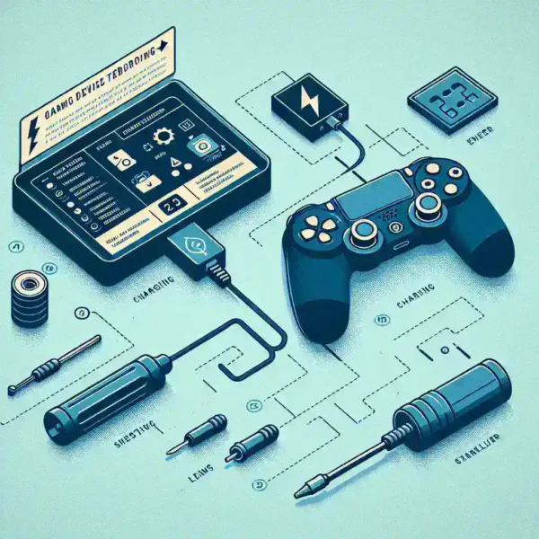
How to Charge Your Nintendo Switch Controllers (+ Troubleshooting Tips)
One of the essential tasks for any Nintendo Switch owner is to keep their controllers charged and ready for gaming. Here’s how you can effectively charge your Nintendo Switch controllers:

How to Make a Video on Snapchat
Snapchat is a popular social media platform known for its disappearing photos and videos. It allows you to connect with friends and share moments in real-time. One of the key features of Snapchat is creating and sharing videos. In this article, we will guide you through the steps of making a video on Snapchat.

The Best YouTube to MP3 Converters for Easy Music Downloads
YouTube is a goldmine of music, and sometimes you just want to have access to your favorite tunes offline. That’s where YouTube to MP3 converters come in handy. These tools let you convert YouTube videos into high-quality MP3 files that you can download and listen to anytime, anywhere.

YouTube Analytics: Unlocking the Power of Data
As a content creator on YouTube, understanding the performance of your videos is crucial. This is where YouTube Analytics comes in – a powerful tool that provides you with valuable insights into the performance and audience engagement of your content.

Video Monetization
With the rise of video content, more and more individuals and businesses are looking for ways to monetize their videos. Whether you’re a content creator on YouTube or a marketer looking to leverage video advertising, video monetization can be a lucrative endeavor.

How to Turn Off AirPlay
In a life where technology seamlessly integrates into our daily lives, AirPlay has become a household term for Apple users. Whether you’re streaming music, movies, or presentations, it’s a fantastic tool. But what happens when you need to switch it off? In this comprehensive guide, we will show you how to turn off AirPlay effortlessly.
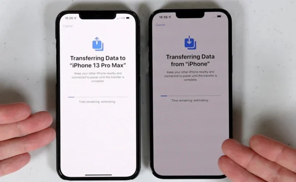
How to Transfer Data to New iPhone
Getting a new iPhone is an exciting experience, but the task of transferring your data can be daunting. Fortunately, with the right guidance and tools, the process can be seamless. In this guide, we’ll explore the various methods for transferring data to your new iPhone. Whether you’re upgrading or switching from an Android device, you’ll find the answers you need.

How to Clear Cookies on iPhone
From connecting with loved ones to accessing information at our fingertips, our iPhones have transformed the way we live. However, with the convenience of digital life comes the necessity to manage our privacy and device performance. One essential aspect of this is knowing how to clear cookies on your iPhone. In this comprehensive guide, we will explore the importance of managing cookies, delve into the step-by-step process of clearing them, and address common FAQs about this crucial task.

How to Download Google Chrome on Mac
Google Chrome is a name that needs no introduction. It’s fast, secure, and packed with features that enhance your browsing experience. In this comprehensive guide, we’ll walk you through the process of downloading and setting up Google Chrome on your Mac. From system requirements to troubleshooting common issues and customizing your browser, we’ve got you covered.

How to Restore Contacts on iPhone
Contacts hold the key to our personal and professional networks. Losing them can be a real hassle. But fear not! In this comprehensive guide, we will explore the ins and outs of how to restore contacts on iPhone. Whether you accidentally deleted contacts, switched devices, or encountered a technical glitch, we’ve got you covered. We will walk you through the entire process, sharing insights, tips, and tricks to ensure your contact list remains intact.

How to Download Instagram Videos
What if you come across a captivating video on Instagram that you’d like to save for offline viewing or share with friends? In this comprehensive guide, we’ll show you how to Instagram video download easily and legally, while respecting the platform’s terms of use. Whether you’re tech-savvy or a beginner, we’ve got you covered with step-by-step instructions and expert tips.

Quick Guide: How to Restart Your Apple Watch for Optimal Performance
Restarting your Apple Watch can be a simple yet effective solution to address minor glitches, improve performance, or resolve connectivity issues. In this guide, we’ll walk you through the easy steps to restart your Apple Watch, ensuring that it functions smoothly and provides you with a seamless wearable experience.

Choosing the Best iPad for College: A Comprehensive Guide
Selecting the right iPad for college can significantly enhance your academic experience, providing you with a powerful tool for note-taking, research, and multimedia consumption. In this guide, we’ll explore key considerations and recommend the best iPads suited for college students, taking into account performance, features, and budget constraints.

Boosting Cardio Fitness: A Guide for Improving Low Cardio Fitness with Apple Watch
Apple Watch is not only a stylish accessory but also a powerful fitness companion that can help improve your cardiovascular health. If your cardio fitness level is lower than desired, this guide will show you how to leverage the features of your Apple Watch to enhance your cardiorespiratory fitness and lead a healthier lifestyle.

Navigating the Roads: Apple Maps vs. Google Maps – A Comprehensive Comparison
Choosing the right navigation app is crucial for seamless and efficient travel experiences. Apple Maps and Google Maps stand as two prominent contenders in the world of navigation apps, each offering distinct features and advantages. In this comprehensive comparison, we’ll explore the strengths and weaknesses of Apple Maps and Google Maps to help you make an informed decision based on your preferences and needs.

Unlocking Creativity: A Guide to TikTok Video Downloaders
TikTok, the vibrant and creative video-sharing platform, has become a hub for content creators worldwide. If you’ve come across a TikTok video that you wish to save for offline viewing or share with friends, a TikTok video downloader can be a valuable tool. In this guide, we’ll explore the concept of TikTok video downloaders, their functionalities, and the considerations to keep in mind when using them.

Troubleshooting Guide: Why Your iPad May Not Be Charging and How to Fix It
Encountering issues with charging your iPad can be frustrating, disrupting your usage and productivity. This troubleshooting guide aims to address common reasons why your iPad may not be charging and provides step-by-step solutions to help you identify and resolve the issue.

Navigating Instagram Stories: Understanding the Instagram Story Viewer Phenomenon
Instagram Stories have become a popular and dynamic feature, allowing users to share ephemeral content that disappears after 24 hours. The curiosity surrounding who views your stories has led to the emergence of various Instagram Story Viewer tools and services. In this article, we’ll explore the concept of Instagram Story viewers, the ethical considerations involved, and the impact on user privacy within the Instagram community.

Unveiling Innovation: Exploring the Features of the New Apple AirPods
Apple continues to redefine the audio experience with its cutting-edge technology, and the latest addition to its lineup, the new Apple AirPods, is no exception. In this article, we’ll delve into the exciting features and enhancements that make the new Apple AirPods a must-have for enthusiasts and those seeking an immersive audio experience.